Fixing the routing and starting again with it!
- Session
- 22 of 33
- Date
- 18 May 2026
- Time worked
- 1 h 18 min
- Reading time
- 2 min
- Images
- 7
After switching back to the routing, I firstly had to remove the old routing, remove the old components that I didn't need anymore, and add the new ones. I firstly looked to see if I could do that somehow automatically,
and after going to Edit and then to Global Deletions, I selected tracks and vias and deleted them.
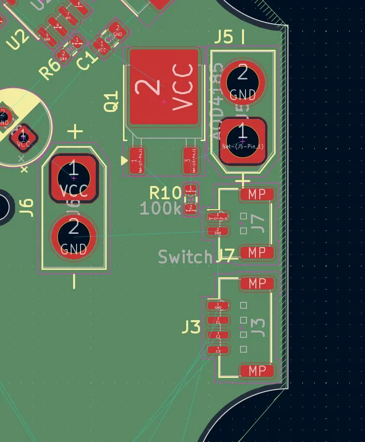
After that, I pressed F8 to load the new pieces and then deleted the old ones manually. After that, I tried placing Q1 as near as possible to the J5 power XT-cable, but then the problem was that the pin 2 Vcc block was always going against the capacitor C1, which made it impossible. But after flipping J5, I got much more space and then I placed the R10 resistor there. The only problem then was that I didn't know where to place J7, which was for the on/off switch, and because I had much space on that side, I decided to move the J5 XT30 to the top and bring the new J7 into the middle, so after all it looked like that:
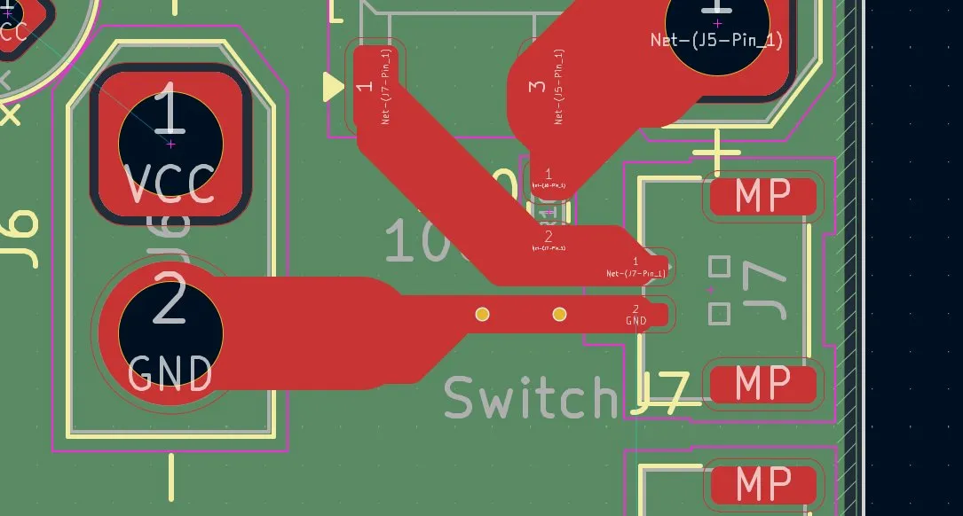
Then I started routing again: Firstly, I connected the + pin of the battery over pin 3 with the resistor and then the other end of the resistor. This line has to be massive, because the whole power of the battery goes through there. Next, I connected pin 1 of Q1 with the other leg of the resistor to the J7 pin 1 again. This one should be big, but not too big, because the max 12.6V for the MOSFET will be there. Lastly, I connected the GND.
So after doing all of that, it looked like that:
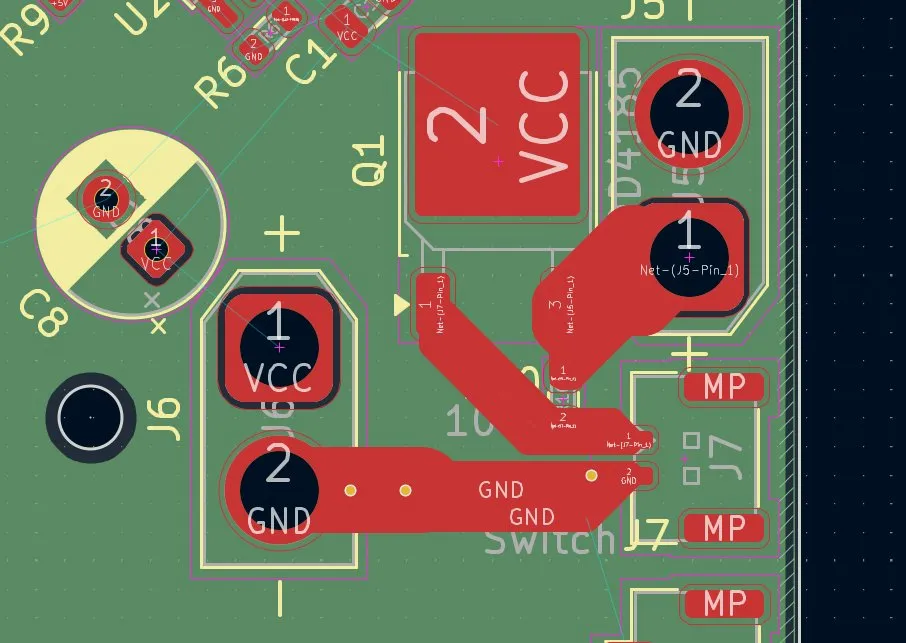
But then I decided to make the GND lane even bigger, so that it flows much better and doesn't heat up that much:
After that, I continued on making the battery percent measurement, but first I thought of moving U3 etc. more closely to the connector:
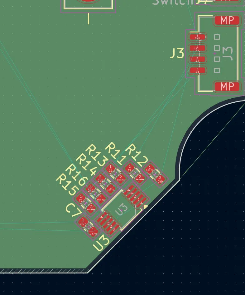
I decided to position it like that because it's the shortest way for SCL and SDA, but also the shortest way to C1, C2, and C3, while also being far away enough to be safe from interference, noise, etc.
And after connecting all parts to the chip and the resistor, it looked like that:
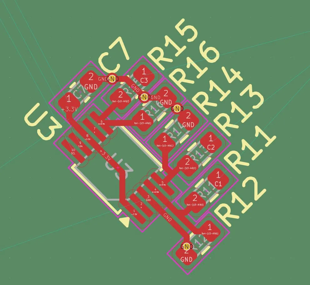
But then I thought that I maybe should move the 3.3V track that is under the U3 chip somewhere else, so that the chip doesn't get noise, etc. After a bit of thinking, I decided to do it with vias and move it to the 3rd layer, the power layer.
And after doing it, it worked perfectly and looked like that:
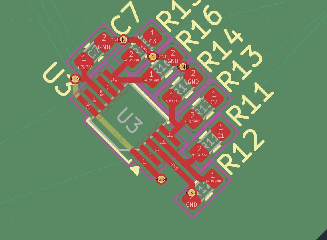
But then I noticed another small problem: the via for 3.3V was blocking the SDA in the future, so I switched it and made it on the other side.
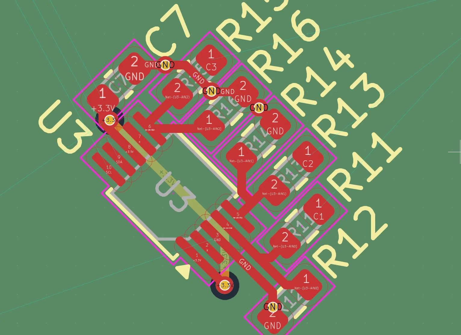
Happy that I got everything working now, it'll be much faster, and I'm happy with the progress.
Session recordings
Timelapse recordings of this session.